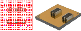
Product introduction:
The GF35303ME-1323 intermediate frequency amplification and filtering chip integrates equalizer chip, gain block chip, filter chip, single pole double throw switch chip, digital attenuator chip, etc. It has achieved functions such as numerical control attenuation, amplification, and filtering of intermediate frequency signals. It is manufactured using silicon-based MEMS technology and multi-layer stacking is achieved through wafer bonding. It is housed in a silicon-based BGA package, suitable for SMT.
principle diagram: 
parameters:
| No. | Index | Symbol | Conditions: Room temperature TA=25℃, working voltage ± 5V, max frequency range: 1.3-2.3GHz | Limit value | Unit | |
| Min | Max | |||||
| 1 | Gain | G_±30MHz | ±30MHz BW | 21 | – | dB |
| 2 | G_±500MHz | ±500MHz BW | 23 | – | dB | |
| 3 | Output P-1 | P-1_±30MHz | ±30MHz BW | 17 | – | dBm |
| 4 | P-1_±500MHz | ±500MHz BW | – | 12 | dBm | |
| 5 | 0.5dB attenuation control | ATT | 6-bit digital control attenuationTTL control,+5V/0V low level effective | 0.35 | 0.65 | dB |
| 6 | 1dB attenuation control | 0.8 | 1.2 | dB | ||
| 7 | 2dB attenuation control | 1.7 | 2.3 | dB | ||
| 8 | 4dB attenuation control | 3.6 | 4.4 | dB | ||
| 9 | 8dB attenuation control | 7 | 9 | dB | ||
| 10 | 16dB attenuation control | 14 | 18 | dB | ||
| 11 | Out-of-band rejection | – | ±30MHz BWDC~1700MHz,1900~10000MHz | 50 | dBc | |
| 12 | – | ±500MHz BWDC~1100MHz,2500~10000MHz | 40 | dBc | ||
| 13 | RF port standing wave | VSWR | – | – | 2.2 | – |
| 14 | VDD current | I_VDD | – | – | 250 | mA |
| 15 | VEE current | I_VEE | – | – | 20 | mA |
IF Amplification and Filtering Chip

